National Academy of Sciences of Ukraine
Scientific Center "Institute
for Nuclear Research"
Department
of Plasma Physics, Kiev, Ukraine
Prof.
G.S. Kirichenko
Prof. V.A. Saenko
Dr. A.G. Borisenko |
Know
 How! How! |
The
new type of the plasma source and the thin film deposition technology
on the basis of the Arc Discharge in the Vapors of the Anode Materials
(ADVAM) |
 Thin
Films Deposition Technology Thin
Films Deposition Technology
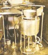
The new type of the plasma source and the thin film deposition technology
on the basis of the arc discharge in the vapors of the anode materials (ADVAM)
were constructed. The previous studies as well as the tests of plasma source
models have shown, that:
- It is possible to produce the films with
a large adhesion on substrates from different kinds of materials without
the use of additional sub-layers ensuring the needed adhesion level,
in particular the films of copper on Si, SiO2, and others.
- Ion part in a plasma flow of a source
can be regulated from 10 % up to 80 % depending on the chosen mode of
work, working material and constructional features of a used plasma
source. In particular, for a copper plasma flow the part of ions in
a flow equals up to 35 %, and for Ti it reaches 85 %. This allows to
create technological modes with the self-sputtering of deposited films
by ions of the plasma flow itself.
- It was found with the help of a reverse
Rutherford scattering technique that the amount of impurities in deposited
copper films at different operating plasma source modes does not exceed
0.05 %. Use of high-quality copper mirrors with reflection factor of
99.2 % which were manufactured with the help of our methods, confirms
these data.
- Our studies have shown that by a choice
of the appropriate mode of a plasma source operation, it is possible
to regulate as a value of an insulated dielectric substrate floating
potential, as the energy reaching the ion substrate, and by this way
to avoid or considerably reduce the quantity of defects in deposited
films or in superficial layers of a substrate.
Practical
applications.
With the help of this source
- high-quality copper laser mirrors with
reflection factor of 99.2 % (
l =1.315
microns),
- contrast x-ray photo masks,
- high-quality functional, conducting, contact
and barrier layers in microelectronics,
- conducting layers and executive elements
in micromechanics,
- a series of protective and decorative
coverings, including coverings of multicomponent structure were created
and used.
 Possible
practical use of the offered development. Possible
practical use of the offered development.
Offered for development plasma sources can be applied for:
- Technological operations in manufacturing
the microcircuits of sub-micron technologies in which absence of a drop
phase in the flow, fraction of ions in it, presence of a compensated
flow volumetric charge are extremely important. The source can effectively
be used in the new "know-how" of microcircuits with different purposes,
and with the use of copper instead of aluminium.
- Deposition of high-adhesive films of
a wide series of materials (Cu, Ni, Cr, Ti, Ta, Nb, Mo, W, U,
 Au,
Ag and others) and coverings of different purposes on dielectric, semi-conductor
and metal substrates (including copper films ) without additional sub-layers.
Deposition of high-adhesive sub-layers. Deposition of superthin films. Au,
Ag and others) and coverings of different purposes on dielectric, semi-conductor
and metal substrates (including copper films ) without additional sub-layers.
Deposition of high-adhesive sub-layers. Deposition of superthin films.
- Deposition of films and coatings which
can simultaneously and purposefully influence on their properties due
to the controlled change of ion component parameters in a deposited
plasma flow without introducing additional harmful impurities in the
film structure.
- Realizations of technological modes with
regulated self-sputtering of deposited by ions films in the used plasma
flow. Such modes can represent a basis of new technological processes
of conducting copper layers formation in manufacturing the microcircuits
of sub-micron technology.
- Deposition of films and coatings based
on intercompounds of metals with gases: nitrides, oxides, borides and
others.
 This
plasma source was successfully used for the high-adhesive films production
for various aims: high-quality copper laser mirrors; contrast x-ray masks;
high-quality functional, conducting, contact and barrier layers for microelectronics;
conducting layers and executive elements in micromechanics; a number of
protective and decorative coverings, including multicomponent coverings. This
plasma source was successfully used for the high-adhesive films production
for various aims: high-quality copper laser mirrors; contrast x-ray masks;
high-quality functional, conducting, contact and barrier layers for microelectronics;
conducting layers and executive elements in micromechanics; a number of
protective and decorative coverings, including multicomponent coverings.
APPLICATIONS
Technological processes of microelectronics, micromechanics, precision
instrument manufacture, deposition of protective, hardening, corrosion-resisting
and decorative coatings.
This plasma source can generate macroparticle-free plasma flows of various
substances with controllable ion energies, starting Ei ( 50 eV, to form
functional layers with minimum structural defects and high adhesibility.
High fraction of ions in flow allows one to directly process the growing
covering by ions of deposited material without use of ions of other chemical
elements, thus increasing purity and quality of films.
The sources are estimated to be applicable for manufacturing of copper
films, instead of aluminum films, in microelectronics. Operation modes
with controlled self-sputtering of deposited films by ions may be especially
useful for producing of conducting copper layers in manufacturing of microcircuits
with sub-micron patterns.
It can be used for vacuum deposition of high-adhesive thin films of metals
with different melting temperatures and chemical activities in melted
state. Also, for deposition of thin films of complex composition (oxides,
nitrides, and carbides), during the pure-gas discharge the source is used
to carryout the final ion refinement of substrates justs before the thin
film deposition.
The source is compatible with any standard equipment, it is intended for
thin film deposition.
SPECIFICATIONS
|
Total consumed power,
kW
|
.3 to 5 |
|
|
|
Arc current range,
A
|
.2 to 10 |
|
|
|
Range of voltage drop
at the arc, kV
|
0.2 to 0.8 |
Density of ion current
on the substrate, mA/cm2
|
to
2. |
|
Range of voltages at
the additional anode,kV
|
0.1 to 0.5 |
Diameter of plating
area, mm
|
150 |
|
Magnetic field intensity,
kA/m
|
8 to 12 |
Film in thickness inhomogeneity
in plating area, %
|
±10 |
|
Rate of evaporation
of working substance,mg/s
|
0.3 to 0.5 |
Working substance
|
Ti, Ni, Cu, Cr, Al, Ta, Nb, C,
Mo, W |
|
Degree of substance
ionization in the flow, %
|
to 85 |
|
|
Rate of the thin film
deposition at stationary exposition of substrates, nm/s
|
0.1 to 2 |
Dimensions, mm:
diameter x height
|
170 x 200. |
|